Through-Hole PCB Assembly2026-04-17T06:32:59+00:00

Reliable Through-Hole PCB Assembly Solutions for Durable Electronic Applications

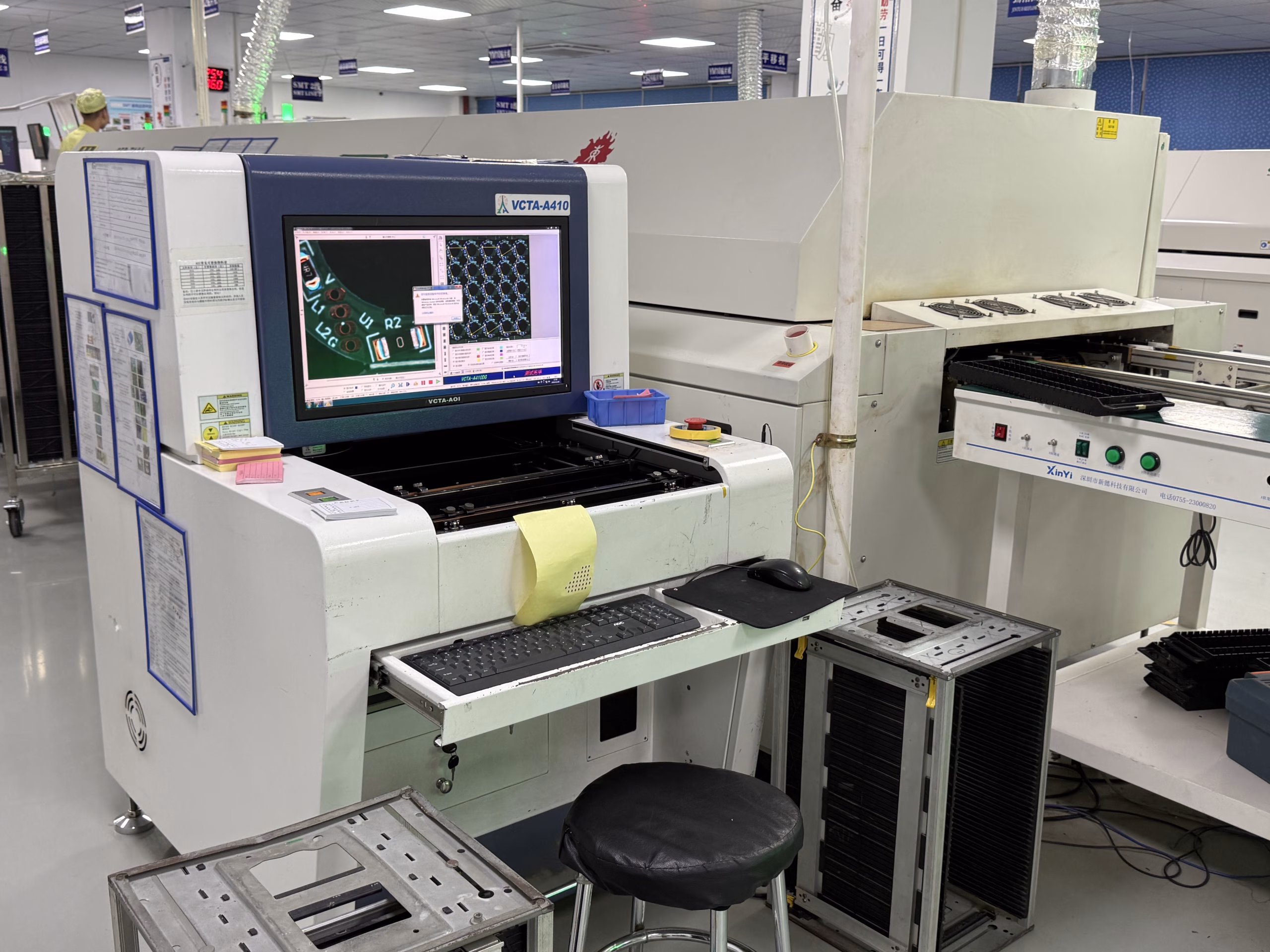
OrinewPCB provides through-hole PCB assembly for electronic products exposed to mechanical or environmental stress. We offer manual and automated through-hole assembly to support prototype, low-volume, and high-volume production.

  • IPC 610, ISO 9001, RoHS compliance
  • Full through-hole assembly services from prototype to high-volume production

  • Manual and automated insertion for axial, radial, and large components

GET YOUR QUOTE!

Click or drag a file to this area to upload.

What is Through-Hole PCB Assembly?

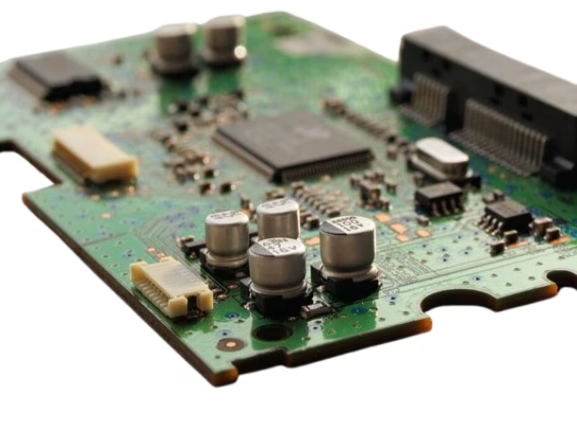
Through-hole PCB assembly is a process where components are inserted through holes drilled into the printed circuit board and soldered to pads on the opposite side. This technique forms strong mechanical and electrical bonds between the circuit and its components, providing high durability for applications subjected to vibration, heat, and high voltage.

Unlike surface mount technology, which mounts components directly onto the board surface, through-hole assembly secures component leads deep within the board structure. This makes it suitable for heavier components, such as transformers, capacitors, and connectors, where mechanical strength is required.

Our Through-Hole PCB Capabilities

OrinewPCB supports axial components, radial components, and through-hole components, including transformers, inductors, and large connectors. We provide manual and automated insertion, with automated insertion for volume PCB assembly and manual soldering or selective soldering for prototypes and complex boards. This ensures accurate component placement and secure component leads for assemblies subjected to mechanical or environmental stress.

We assemble single-sided, double-sided, and multilayer printed circuit boards with up to 64 layers. Designs can integrate through holes with SMT components for hybrid circuit board assembly, combining mechanical strength with space efficiency. Our construction supports PCB through-hole designs for high voltage, thermal cycling, and vibration durability.

Surface finishes include ENIG, HASL, OSP, immersion silver, and immersion tin, selected based on PCB assembly requirements and assembly techniques. We work with substrates such as FR4, high TG FR4, halogen-free laminates, and Rogers HF materials, offering heat tolerance and mechanical stability under environmental stress and high power conditions.

Our assembly process supports copper thicknesses ranging up to 1000 μm. This flexibility increases current-carrying capacity and heat tolerance, especially in high-voltage power supplies, industrial control systems, and automotive electronics. The heavier copper also provides stronger bonds between the circuit and components, improving mechanical resilience.

We source electronic components from trusted distributors such as Mouser, Digi-Key, Future Electronics, and WPG Holdings. Our PCB assembly process includes component placement, insertion through holes drilled in the board, manual and automated soldering, optical inspection, functional testing, and final quality verification. We offer full PCB assembly capabilities, covering prototype through volume production.

Our testing protocols include functional testing, optical inspection, and electrical testing using oscilloscopes, signal generators, programmable digital power supplies, and high-voltage testers. We also apply automated optical inspection (AOI), X-ray inspection, and assembly testing. All work is performed to IPC 610 Class 2 and Class 3 standards.

Where is Through-Hole Assembly Used?

Power Supplies and High Voltage Circuits

Through-hole assembly supports high-voltage components such as transformers, large capacitors, and inductors. The process forms stronger bonds between

the circuit and the component leads, offering the heat tolerance and mechanical durability required for power electronics.

Automotive Control Modules

In automotive applications, through hole PCB designs secure heavier components that experience constant vibration and temperature fluctuations. This

assembly method reduces the risk of mechanical failure compared with surface mount technology.

Industrial Control Systems​

Industrial equipment often faces mechanical or environmental stress. Through-hole assembly offers stronger mechanical connections for circuit boards

used in control panels, robotics, and machinery operating in demanding environments.

Medical Electronics​

Medical devices use through hole PCB assembly where reliability and resistance to environmental stress are important. The ability to handle high

voltage and maintain stable electrical connections makes it ideal for life-supporting and diagnostic equipment.

Aerospace and Defense Systems​

Through-hole technology is chosen for circuit board assembly services in aerospace and defense, where assemblies must endure mechanical shock,

vibration, and extreme temperatures while maintaining performance.

What are the Benefits of Through-Hole PCB Assembly?

Stronger Mechanical Bonds

Through-hole assembly creates stronger bonds between the circuit and component leads. By inserting leads through drilled holes and soldering them onthe opposite side of the board, this method resists mechanical stresses such as vibration, shock, and repeated movement, making it suitable for mechanical or environmental stress conditions.

Higher Heat and Power Tolerance

Through-hole technology offers superior heat tolerance and the ability to handle high voltage and high current loads. The robust connections canwithstand temperature cycling and power surges, which is important in power supplies, automotive systems, and industrial controls where heavier components are used.

Support for Large and Heavy Components

Unlike surface mount technology, which is limited to smaller, lighter parts, through-hole assembly supports large components, including transformers,inductors, capacitors, and heavy connectors. This flexibility expands design options for applications requiring high durability and current handling.

Improved Durability Under Environmental Stress

Through-hole PCB assemblies maintain electrical and mechanical performance even in challenging environments. Assemblies are more resistant to environmental factors like humidity, vibration, and thermal cycling, ensuring long-term reliability in automotive, industrial, and medical electronics.

Compatibility wtih Mixed Technology Designs

Through-hole assembly integrates smoothly with SMT components in mixed-technology designs. This allows engineers to combine the mechanical strength of through holes with the space efficiency of surface mount technology, optimizing circuit board assembly services for both durability and compact layouts.

Our Through-Hole PCB
Testing Process

OrinewPCB applies a comprehensive testing and inspection process to confirm electrical performance, mechanical reliability, and solder joint integrity in every through-hole PCB assembly. We apply testing protocols based on the IPC 610 Class 2 and Class 3 workmanship standards, which specify acceptance criteria for solder joint quality, component placement accuracy, and mechanical durability.

Functional Testing

Functional testing verifies that the assembled circuit and its components perform according to design specifications under normal and stress conditions. We simulate operating environments and apply expected voltage and current levels to detect faults such as open circuits, shorts, or signal loss.

Optical Inspection

Optical inspection includes manual visual checks and automated optical inspection (AOI). AOI systems use high-resolution cameras and pattern recognition software to detect missing components, improper component placement, misalignments, insufficient solder joints, and surface defects. This allows early detection of process variations before final testing.

Electrical Testing

Electrical testing involves using oscilloscopes, signal generators, programmable digital power supplies, and high-voltage testers. These tools measure parameters such as voltage stability, current carrying capacity, and signal continuity, important for high voltage and heat tolerance applications where through-hole technology is preferred.

X-ray Inspection

At OrinewPCB, we use X-ray inspection to examine hidden solder joints, internal vias, and plated through holes. This non-destructive technique identifies voids, bridging, or cold solder joints that may not be visible externally but can impact long-term reliability.

Assembly Testing

Assembly testing confirms the integrity of the assembly process, validating that components are inserted through holes drilled accurately and soldered to meet mechanical strength requirements.

Through Hole vs SMT Assembly

Feature

Through-Hole Assembly

Surface Mount Technology(SMT)and soldered to surface pads.

Component Mounting

Components are inserted through holes drilled into the board and soldered to pads.

Components are placed directly onto the PCB surface and soldered to surface pads.

Mechanical Strength

High. Leads create stronger bonds between the circuit and component leads, suited for mechanical or environmental stress.

Lower. Reliant on surface solder joints, which may be weaker under vibration or stress.

Component Types

Supports axial and radial components, large components, and those with high voltage or heat tolerance needs.

Best for smaller, lighter components where space savings and automation are priorities.

Assembly Process

Manual and automated insertion, manual soldering, or selective soldering.

Fully automated placement and SMT PCB assembly with reflow soldering.

Applications

Power electronics, automotive, medical, aerospace, industrial control systems.

Consumer electronics, compact devices, high-speed digital circuits.


Why Choose OrinewPCB as Your Through_Hole PCB Assembly Service Provider?

Proven Track Record and Industry Experience

Since 2007, OrinewPCB has delivered reliable PCB assembly solutions to over 3,000 customers worldwide.

Our experience spans industrial, automotive, medical, and aerospace sectors, giving us the expertise to meet the demands of complex circuit board assembly services.

Certifications and Quality Compliance

Our assembly process follows IPC 610 Class 2 and Class 3 workmanship standards. We also maintain ISO 9001, IATF 16949, and RoHS compliance across all production.

These certifications confirm that our assembly services meet strict quality control and environmental standards required by the automotive, medical, industrial, and aerospace sectors.

Original Component Sourcing for Reliability

We source electronic components exclusively from authorized distributors, including Mouser, Digi-Key, Future Electronics, and WPG Holdings.

This prevents counterfeit parts from entering your PCB assembly process, maintains traceability, and confirms consistent quality across every build.

Production Flexibility and Fast Lead Times

We support prototype, small-volume production, and volume PCB assembly, offering flexibility for both development and full-scale manufacturing.

Our quoting process delivers responses within 8 working hours for bare boards and 2 working days for PCB assembly service quotes. Lead times range from 4 to 25 days, depending on design complexity and production volume.

Engineering Support and Design Assistance

OrinewPCB provides comprehensive design support, including PCBA review, component selection, impedance matching calculations, and production process evaluation.

These services help optimize assembly techniques and confirm that designs meet industry standards while aligning with your PCB assembly requirements.

Full-Service Manufacturing Under One Roof

Our PCB assembly capabilities are integrated with PCB manufacturing, component sourcing, wire harness fabrication, and conformal coating.

This end-to-end service reduces supplier coordination time and improves quality control throughout the assembly process.

All production takes place in our two fully equipped PCBA factories located in Shijiazhuang and Shenzhen, China, covering more than 10,000 square meters.

Through_Hole PCB Assembly | FAQs

Choose through-hole assembly when the design involves heavier components, high heat tolerance, or when the circuit and its components face vibration, thermal cycling, or environmental stress. It is also preferred for high-voltage circuits and assemblies requiring stronger bonds between the circuit and the components.

Yes. Through-hole technology and surface mount technology are often combined in mixed-technology designs. This approach allows through-hole components to provide mechanical strength while SMT components save space and support automated assembly for lighter parts.

Selective soldering applies solder precisely to through-hole components without exposing the entire circuit board to high temperatures. This reduces thermal stress, prevents solder bridging, and improves joint consistency, especially when working with automated through-hole PCB assembly or boards combining through holes and SMT components.

Automated insertion uses precision machinery to place axial and radial components into pre-drilled holes at high speed. This increases placement accuracy, reduces manual handling, and shortens the assembly process for volume PCB assembly, improving production efficiency without sacrificing mechanical strength.

Get Free Quote

Do you need help with PCB, PCB assembly, or electronic components? You can fill out and submit the form to leave your contact information (“*” indicates required fields)

GET YOUR QUOTE!

Click or drag a file to this area to upload.
Go to Top