Reliable Power Bank PCB Assembly Solutions
OrinewPCB specializes in the design, fabrication, and assembly of high-performance power bank PCBs engineered for efficient voltage conversion, robust circuit protection, and seamless integration of fast charging protocols (PD, QC 3.0) across diverse configurations, including 5V, Type-C USB, and multi-cell 18650 battery packs, supported by professional custom cable assembly solutions.
What is a Power Bank PCB?
A power bank PCB (printed circuit board) is the central platform for power storage, voltage conversion, and energy delivery in portable charging devices. It integrates control logic, power regulation, protection circuitry, and interface components, enabling safe and efficient charging and discharging cycles.
Key functions of a power bank circuit board include:
- Voltage Step-Up Conversion: Boost converter circuits increase the lithium battery voltage (typically 3.7V nominal) to output levels such as 5V, 9V, 12V, or 20V, depending on the device’s requirements.
- Current Regulation: Controls output currents commonly ranging from 1A and 2A up to high-power profiles (20W, 65W, 100W), including fast charging protocols (PD, QC 3.0, 20W fast charging).
- Battery Management: Manages charging and discharging processes, often incorporating balancer circuits for multi-cell packs (like 18650 cells) to optimize cell health and longevity.
- Protection Systems: Provides safeguards against overcharge, over-discharge, overcurrent, short-circuit, and thermal overload conditions.
- Interface Support: Accommodates a variety of connectors, including dual USB, Type-C USB, micro USB, and legacy USB-A ports.
Modern power bank PCBs also support intelligent features such as load detection, LED display status indicators, and compatibility with emerging charging standards like USB-C, PD QC, and QC 3.0 for enhanced efficiency and user safety.

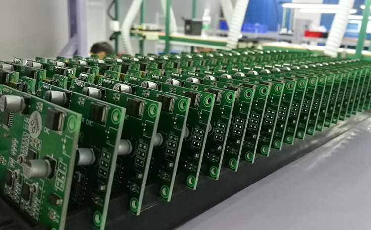
Our Manufacturing Capabilities
OrinewPCB delivers power bank PCB solutions using advanced fabrication methods, precision assembly processes, and comprehensive quality control to meet the demanding requirements of portable power applications. Our facilities support the complete production cycle, from prototype development to high-volume manufacturing.
Features of Monitor PCBs
A power bank PCB integrates primary and supporting components that work together to manage power input, storage, regulation, and output while ensuring safety and efficiency.
LEDs / Display
Provides visual feedback for charge status, output voltage, and error indicators (LED display, LEDs).
Thermal Sensors
Monitors temperature to trigger cooling or shutdown in case of thermal overload.
Why Choose OrinewPCB As Your Power Bank PCB Fabrication Provider?
Types of Power Bank PCB Comparison
|
PCB Type |
Max Current Handling |
Thermal Performance |
Size Efficiency |
Cost Index |
Fast Charging Support |
|
Standard Power Bank PCB |
Up to 2A |
Moderate (FR-4, 1-2 oz copper) |
High |
Low |
Basic (5V 1A/2A only) |
|
Fast Charging PCB (PD/QC) |
3A – 5A (up to 100W) |
High (FR-4 or Polyimide, 2-4 oz copper) |
Medium |
Moderate |
PD, QC 3.0, QC 4.0, 20W to 100W |
|
High-Capacity PCB |
5A+ |
Very High (Polyimide or Aluminum, up to 5 oz copper) |
Variable |
High |
PD QC, Smart Load Detection |
|
Rugged/Industrial PCB |
3A – 10A |
Very High (Aluminum or reinforced Polyimide) |
Lower |
Higher |
Custom fast charging protocols |
Common Power Bank PCB Materials
Selecting the appropriate materials is critical to ensuring the power bank PCB delivers reliable performance, thermal stability, and durability, especially under varying current loads and operating environments.
Power Bank PCB | FAQs
Get Free Quote
Do you need help with PCB, PCB assembly, or electronic components? You can fill out and submit the form to leave your contact information (“*” indicates required fields)