High-Frequency,Low-Loss PTFE PCB Assembly Solutions
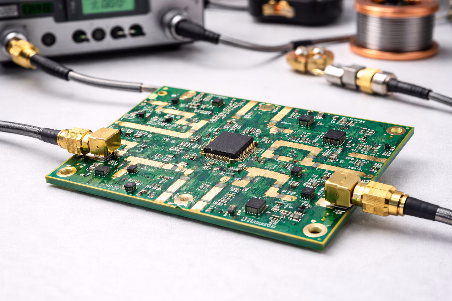
OrinewPCB provides precision PTFE PCB assembly for high-frequency applications requiring mechanical stability, low dielectric constant, chemical resistance, and tight tolerances for performance and reliability. We assemble PTFE PCBs designed for consistent signal integrity and minimal signal loss across wide temperature and frequency ranges.
What is PTFE?
PTFE, or polytetrafluoroethylene, is a synthetic fluoropolymer used as a PCB material in high-performance PCB manufacturing and PCB assembly. Its unique electrical properties, including a low dielectric constant between 2.17 and 2.40 and a low dissipation factor below 0.0015 at 10 GHz, allow PTFE PCB substrates to maintain signal integrity and minimize signal loss in high-frequency applications.
The chemical structure of polytetrafluoroethylene or PTFE provides non-reactivity, high thermal stability, and a low coefficient of friction, making it ideal for PCB fabrication requiring stability across wide frequency ranges and temperature extremes.
PTFE offers exceptional resistance to moisture absorption, with rates typically below 0.01 percent. This protects PCB assemblies from dielectric instability and performance degradation in humid environments. The material’s coefficient of thermal expansion can reach up to 200 ppm/°C, which presents difficulties in processing but can be managed with precise assembly techniques, including controlled lamination and specialized solder processes. Our assembly processes manage PTFE’s low surface energy and high thermal expansion coefficient, reducing delamination risks and solder joint failure.
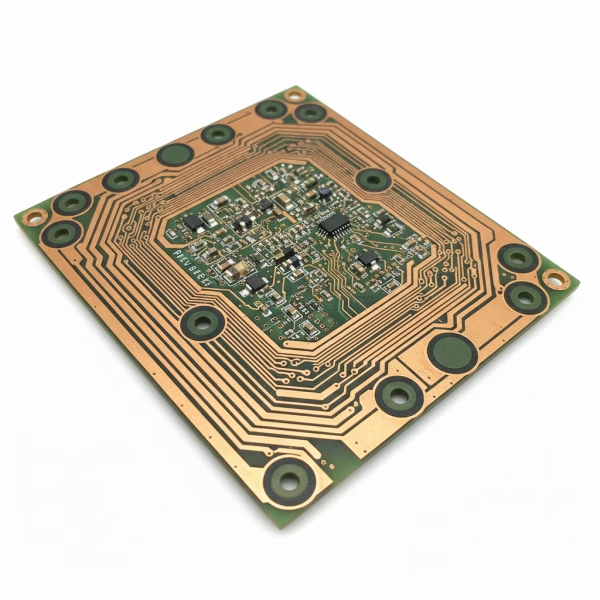
PTFE PCBs are often laminated with copper to provide stable conductor paths while preserving excellent electrical properties for RF and microwave applications. We work with leading PTFE laminates including Rogers, Taconic, Arlon, and other PTFE substrates to ensure optimal performance for your specific application requirements.
Our PTFE PCB Assembly Capabilities
Where are PTFE PCBs Used?
Why Choose OrinewPCB for Your PTFE PCB Assembly?
How does PTFE Compare to Other PCB Materials?
PTFE PCB assembly offers performance advantages over standard materials like FR4 and ceramic-based substrates, particularly for high-frequency applications.
|
Property |
PTFE |
Rogers (RO4350B / RO3003) |
Arlon (AD255C / CuClad) |
Isola (IS620 / IS680) |
Taconic (RF-35 / TLY-5A) |
FR4 |
Ceramic Substrates |
|
Dielectric Constant |
2.17 – 2.40 |
3.38 (RO4350B) to 3.00 (RO3003) |
2.55 (AD255C) to 2.17 (CuClad) |
3.38 (IS680) to 3.45 (IS620) |
2.20 (RF-35) to 2.17 (TLY-5A) |
4.2 – 4.7 |
6.0 – 10.0 |
|
Loss Tangent |
< 0.0015 |
0.0037 (RO4350B) to 0.0010 (RO3003) |
0.0015 (AD255C) to 0.0009 (CuClad) |
0.0035 (IS680) to 0.0050 (IS620) |
0.0018 (RF-35) to 0.0011 (TLY-5A) |
0.018 – 0.025 |
0.0005 – 0.003 |
|
Moisture Absorption |
< 0.01% |
< 0.06% |
< 0.04% |
< 0.10% |
< 0.02% |
0.10% – 0.20% |
Negligible |
|
Processing Complexity |
Advanced lamination and surface treatments are needed |
Requires advanced lamination and surface treatments |
Requires advanced lamination and surface treatments |
Requires advanced lamination and surface treatments |
Requires advanced lamination and surface treatments |
Standard PCB fabrication |
Difficult, requires specialized tooling |
|
Cost Cost |
Higher |
Higher |
Higher |
Higher |
Higher |
Lower |
Higher |
|
Use in High Frequencies |
Ideal for high-frequency applications |
Ideal for high-frequency applications |
Ideal for high-frequency applications |
Ideal for high-frequency applications |
Ideal for high-frequency applications |
Limited by dielectric loss |
Suitable but expensive |
Teflon PCB Fabricator | FAQs
Get Free Quote
Do you need help with PCB, PCB assembly, or electronic components? You can fill out and submit the form to leave your contact information (“*” indicates required fields)